
Precision CNC Machining for Semiconductor Equipment Components
We manufacture high-precision custom components for semiconductor manufacturing equipment — including wafer handling systems, process chambers, lithography tooling, and inspection fixtures. With ±0.01mm tolerances, 3-5 day rapid prototyping, and full MES traceability, we support your mission-critical semiconductor projects from prototype to production.
Semiconductor Equipment Component Manufacturing Capabilities
We deliver high-precision custom-machined components specifically for semiconductor manufacturing equipment — wafer handling systems, process chambers, lithography tooling, and inspection fixtures. Every project follows our full quality-control workflow, from raw material incoming inspection through final dimensional verification. We machine a wide range of materials including aluminum alloys, stainless steels, tool steels, copper alloys, and engineering plastics — detailed material capabilities are listed below. With 3 CNC machining centers, wire EDM, surface grinders, and precision inspection equipment including Nikon projectors and TESA height gauges, we ensure consistent quality across every batch. Our MES-based production tracking provides full traceability from raw material to final shipment. No minimum order quantity — we treat every part with the same rigorous quality standards.
±0.01mm Precision
Critical dimensions held to ±0.01mm tolerance, verified on Nikon profile projectors and TESA height gauges
3-5 Day Rapid Prototyping
Fast-turnaround prototype machining for semiconductor R&D and equipment maintenance
Full MES Traceability
Every part traceable to machine, operator, and inspection records via Heihu MES system
Typical Semiconductor Equipment Components We Machine
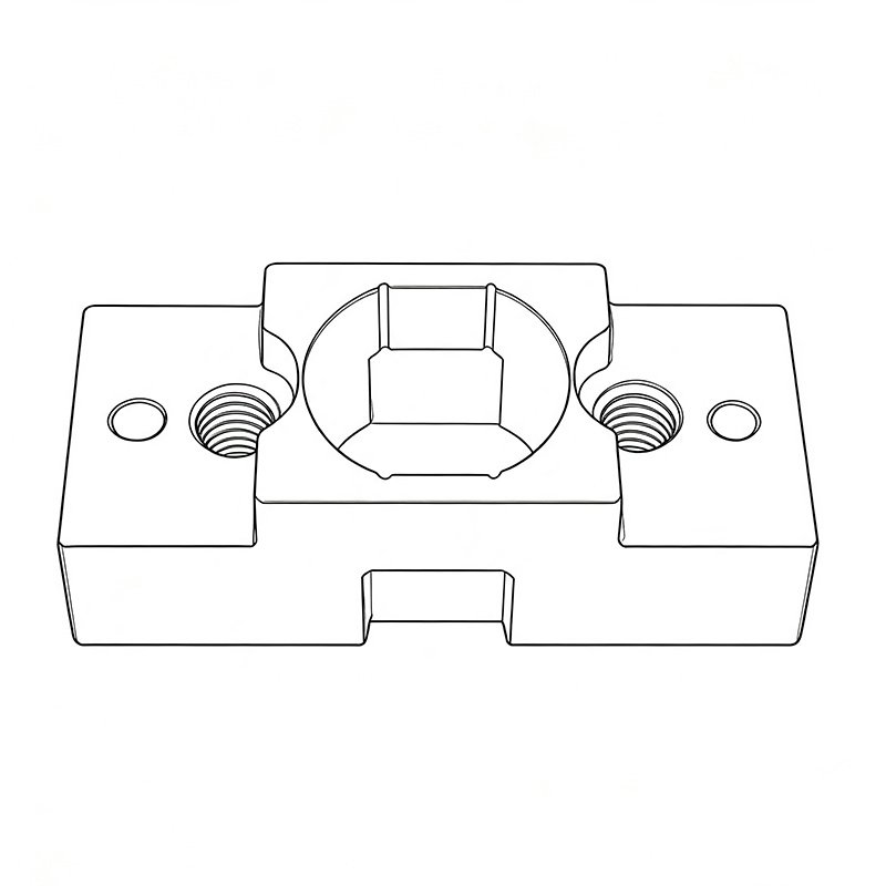
Semiconductor Precision Adapter
440C stainless steel (HRC58) (equivalent to 1.4125 / SUS440C)
±0.005mm precision, Ø2mm bore (+0.012 / +0.015) tolerance
High-hardness precision adapter for semiconductor tooling
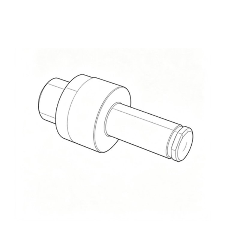
Semiconductor Positioning Drive Shaft
D2 tool steel (equivalent to 1.2379 / SKD11) HRC58
±0.01 mm, ENP surface treatment Φ10 × 25 mm
High-hardness positioning drive shaft for semiconductor packaging & test equipment
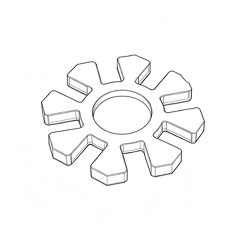
Semiconductor-Grade Precision Coils
PEEK (semiconductor-grade)
±0.2mm, thin-wall precision
Insulation & sealing parts for semiconductor equipment
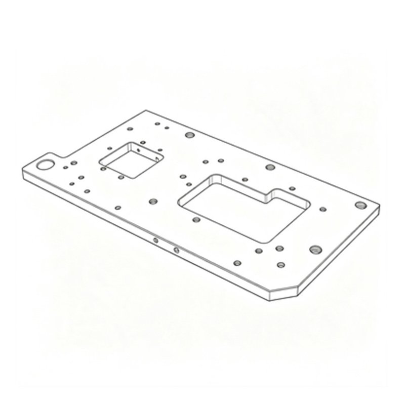
Semiconductor Fixture Base Plate
S235JR carbon steel (equiv. AISI 1018)
±0.01mm, ENP surface treatment
Semiconductor packaging & test equipment mounting platform
Our Semiconductor Equipment Component Manufacturing Capabilities
Aluminum Alloys
6061 · 7075 · MIC-6 · 2017A · EN AW-2017 · A6061 · A6061T6 · A7075 · AlMg2.5
Stainless Steel
SUS304 · SUS316L · 17-4PH · 440C · 303 · 1.4305 · 1.4301 · 1.4125 · 1.4528 · 3.3211 · 3.4365 · 3.3523
Tool & Die Steels
1.2379 · 1.2344 · 1.0503 · 1.173 · 1.1545 · 1.0037 · 1.164 · 1.0535 · 1.2510 · 1.2738 · D2 · H13 · O1 · P20 · 1045 · S235JR · X165CrMoV12
Copper Alloys
3.4365 · 3.3523 · 3.3211
Engineering Plastics
POM · PEEK (semiconductor-grade, thin-wall precision)
Additional specialty materials (titanium, Hastelloy, Invar, Kovar) also available upon request.
Our Equipment
3 CNC Centers · Wire EDM · 3 Surface Grinders · Large Surface Grinder · 3 Milling Machines · Tapping · Laser Marking
Inspection Equipment
Nikon Projector · Wanhao 2.5D CMM · TESA HITE 400 · TESA 700 · Nikon MFC 101A · Hardness Tester · Pin Gauges
Quality & Cleanliness Control for Semiconductor Equipment Components
Dimensional Precision
Critical dimensions held to ±0.01mm tolerance, verified on Nikon profile projectors and TESA height gauges
Surface Quality
Surface finishes down to Ra 0.8μm or better, with deburring and edge finishing applied to every part
Deburring & Clean Handling
Deburring to prevent particle generation, clean handling, and clean packaging for every shipment
100% Inspection
Every critical dimension verified before shipment. Actual measured values are marked directly on the 2D drawings and shipped together with every order. Formal inspection reports can also be provided upon request.
Full Traceability
Every part traceable to machine, operator, and inspection records via Heihu MES system — from raw material through final shipment
Trusted by Industry Leaders
Tier 1 supplier for Japanese semiconductor equipment manufacturer. NDAs available for confidential projects
Case Study: Precision Adapter for Semiconductor Manufacturing Tooling
Background
A semiconductor equipment manufacturer required a precision adapter component for their manufacturing tooling system — used in the assembly and positioning of critical process modules.
Challenge
Material: 440C stainless steel (equivalent to 1.4125 / SUS440C)
Hardness requirement: HRC58 (after heat treatment)
Critical bore tolerance: Ø2(+0.012, +0.015) — a 2mm diameter feature with a tolerance band of just 0.003mm
Overall dimensions: 10 × 13 × 32mm (miniature precision part)
Our Solution
CNC precision machining with grinding allowance
Heat treatment to HRC58 followed by precision grinding
100% inspection on Nikon profile projector and TESA height gauge
Full traceability records via Heihu MES system
Result
All critical dimensions met drawing specifications
Hardness consistently achieved at HRC58
Parts passed 100% dimensional inspection
Customer placed repeat orders
Ready to Start Your Semiconductor Equipment Component Project?
Send us your 2D/3D drawings or share your requirements. We’ll provide a competitive quote within 24 hours — no MOQ, full MES traceability, and ±0.01mm precision guaranteed for wafer handling components, process chamber parts, and semiconductor inspection fixtures.